In-House MEMS Chip Fabrication
Agiltron leads the industry in advanced thermal actuated MEMS device design and fabrication. The company operates a 150mm wafer fabrication facility. The 5,000 ft² cleanroom space also serves as a new product development, demonstration, integration, and qualification area for outside customers.
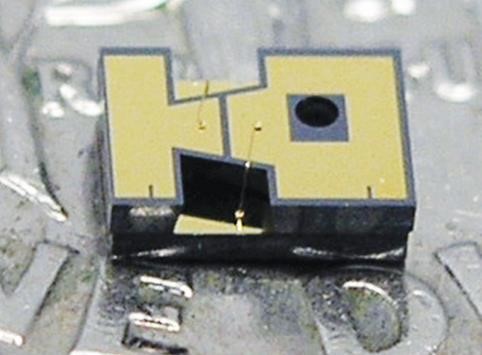
Agiltron produces MEMS chips at our in-house MEMS fab facility, located at Woburn headquarters. This capability allows us to reduce the fabrication cost through tight control of manufacturing yield and quality and continuously improve the performance of our MEMS-based products through the combination of design and process improvements. Moreover, we have developed vision-based automatic wafer testing tools that ensure the dynamic performance and quality of each MEMS chip.

Digital 2D MEMS Technology
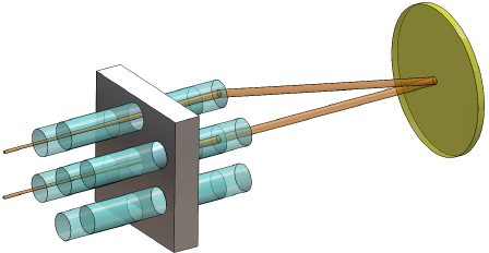
MEMS-based optical switches can be grouped into two approaches: digital 1D and analog 2D. In both cases, micro-mirrors are actuated to redirect light from a given input port to a given output port. In analog 2D switches, a mirror is rotated to obtain the switch function, requiring electronics with firmware to maintain each coupling position. These switches have drawbacks of lost position when power is off and hitless issues in which the signal may leak into unintended channels during switching. The 2D is also unsuitable for inputting light through several ports simultaneously, which may overreach the power threshold and cause damage to the mirror. However, 2D is the lowest for 1xN switch when N>8.

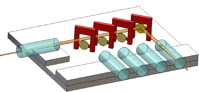
In 1D MEMS switches, each mirror only moves within two positions digitally: in or out of the light path. We use a proprietary thermally actuated digital MEMS offering major advantages of fast switching, direct low driving voltage, fail-safe latching against vibrations, and preserving light paths when power is removed. A typical MEMS mirror arrangement and principle of operation of a digital optical switch is shown in Figure 2.
1D MEMS offers the lowest cost for 1×2, and 2×2 configurations.


Large Motion MEMS Technology
Conventional MEMS are based on electrostatic actuation prone to electrical charge build-up-induced drift and moisture-induced electrical shorting, requiring expensive hermetic sealing. Agiltron’s MEMS is based on the electro-thermal-driven actuation principle. Our unique etMEMSTM design provides advantages for fiber optic components, including:
1. Large actuation force over mm
2. Low direct driving voltage <5V
3. A few fabrication steps, high yield
4. No need for a hermetic package
5. Intrinsic tolerance to EDS
Our MEMS switches and VOAs are based on single crystalline silicon, an exceptional material that does not deform, fatigue, or wear out over time, and its dimensions and mechanical properties are immune to stress unless a critical fracture stress level or a permanent deformation high temperature is reached. Data results from testing show that Agiltron MEMS switches and VOAs still work within specifications after many billion cycles.
